Fujitsu and Socionext Develop Next-Generation 56 Gbps Transceiver Circuit with World's Lowest Power Consumption for Optical Communications between Servers
There is an increasing need to accelerate data transfers between servers in response to improvements in the processing performance of datacenters; however, at the same time, limitations on the amount of electricity that facilities can supply mean that there is also a demand to lower electricity consumption.
Fujitsu Laboratories and Socionext have now developed a new timing detection method that combines the functions of the circuit that compensates signal degradation that becomes prominent as communication speeds improve with some of the functions of the timing-detection circuit that determines the bit-value of input signals, reducing the number of circuits. As a result, they succeeded in developing a 56 Gbps transceiver circuit that achieves twice the speed as before without raising power consumption.
This technology is able to increase the speed of data transfers between chips and optical modules without increasing power consumption, so it is expected to lead to performance improvements in next-generation servers and switches.
Details of this technology will be announced at the IEEE International Solid-State Circuits Conference 2016 (ISSCC 2016), the largest conference related to semiconductor technology, held from January 31 in San Francisco (ISSCC Presentation Number 3.5).
Development Background
In recent years, to support the rapidly expanding needs of cloud computing, there has been a demand for improvements in datacenter processing performance. Datacenters use numerous servers connected through switches to form a large-scale system, and as the processing ability of datacenters has improved, the volume of data exchanged between servers has also been further increasing.
For this reason, there has been progress in international standardization(1) of the communication speed of optical modules used for optical transmission between servers and switches for next-generation datacenters at 56 Gbps, twice current speeds.
At the same time, due to limitations on the amount of electricity that can be supplied in datacenters, there has been a demand for improvements in communication speed without increasing the amount of power consumed by data transceiver circuits.
 Figure 1: Transceiver circuits connecting servers and switches
Issues
Power consumption increases proportionally with communication speed, making it necessary to decrease the power consumed by transceiver circuits in order to boost communication speed without increasing facility power.
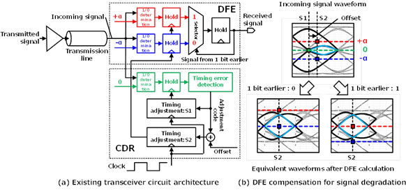
In conventional transceiver circuits, the decision feedback equalizer (DFE), which is a circuit that compensates degraded signals, and the clock and data recovery (CDR) circuit, which detects timing errors between an incoming signal and the internal sampling clock, are responsible for about two thirds of the transceiver circuit's total power consumption, so reducing their power consumption has been a central issue.
For the input-signal waveform that became degraded in the transmission line, the bit value is determined at the determination circuits, one which has a +? threshold value and the other a -? threshold value. The DFE compensates the degraded signal by choosing the determination results of the +? determination circuit if the previous bit value processed was a 1, or the results of -? if the previous bit value processed was 0. The CDR, by observing the incoming signal, adjusts the DFE's operational timing to ensure it captures the signal when the incoming signal's waveform is at its greatest amplitude (Figure 2).
 Figure 2: Existing transceiver circuit architecture and DFE compensation for signal degradation
Larger View (99 KB)
Newly Developed Technology
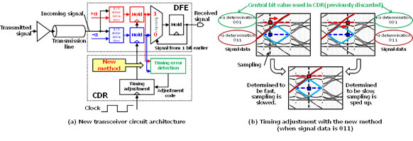
To reduce the power consumption of the CDR, Fujitsu Laboratories and Socionext have now developed a new timing error detection method.
By analyzing waveforms after DFE calculation, Fujitsu Laboratories and Socionext discovered that they could detect whether the DFE's operational timing was early or late by comparing the results of the two DFE determination circuits in cases where three consecutive bits in the input signal were 100 or 011. This led them to develop a new timing detection method that only detects the timing when three consecutive bits of the incoming signal are 100 or 011 (Figure 3).
 Figure 3: New transceiver circuit architecture and timing adjustment with the new method
Larger View (80 KB)
With this newly developed timing detection method, the two companies were able to eliminate the previously required CDR incoming-signal timing-determination circuit, and lines, such as the clock line, which were required as the DFE and CDR operated with different timing. This made it possible for them to succeed in developing transceiver circuitry that doubles speeds to 56 Gbps with the same power consumption as before.
Effects
This new technology will be able to boost data transmission speeds between chips and optical modules without raising power consumption compared to the present. In addition, compatibility with upcoming OIF standards for optical module communications means that optical modules can be expected to be more compact and use less power, requiring half the number of transceiver circuits--from 16 to eight when using this technology--when constructing a 400 Gbps Ethernet with the current 28 Gbps standard.
Future Plans
Fujitsu Laboratories and Socionext will use the newly developed technology in interface components between optical modules and the chips of servers and switches, aiming for commercialization in fiscal 2018.
All company or product names mentioned herein are trademarks or registered trademarks of their respective owners. Information provided in this press release is accurate at time of publication and is subject to change without advance notice.


Комментарии